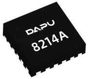
A clock generator produces multiple low-jitter clock signals from a reference clock. The INS8214A is an ultra-low-power clock generator with an integrated fractional-N PLL. It supports multiple reference input types and multiple clock outputs, providing clocking solutions for high-speed systems such as PCIe and Ethernet applications.
Key Features
- Ultra-low power consumption with PLL and buffer operating modes
- Integrated fractional-N PLL with RMS jitter as low as 400 fs (typical, 12 kHz to 20 MHz, Fout = 100 MHz)
- Supports differential, LVCMOS, and crystal reference inputs from 10 MHz to 200 MHz
- Supports four differential clock outputs and one single-ended LVCMOS output
- Supports multiple output formats, including LVDS, LVPECL, LPHCSL, pCML, and LVCMOS
- Supports PCIe Gen1/2/3/4
- Supports spread-spectrum clocking (SSC)
- Supports DCO frequency adjustment with 10 ppb resolution
- Operating temperature range: -40°C to +105°C
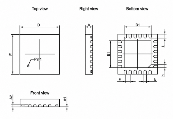
- 24-pin VQFN package, 4.0 mm x 4.0 mm
Applications
- Communications equipment: Ethernet switches, network interface cards, and other networking equipment
- Data centers and servers: PCIe Gen1/2/3/4 systems and multi-clock distribution applications
- Industrial control: MCU-, SoC-, and FPGA-based control systems requiring multiple clock outputs
- Test and measurement: equipment requiring multiple low-jitter clock signals
| Model | Package
Size
(mm) | Reference Input
Frequency | Output
Channels | Output Formats | RMS Jitter
(12 kHz to 20 MHz) | Operating
Temperature
(℃) |
|---|
| INS8214A | 4.0*4.0 | 10 MHz to 200 MHz | 4 differential
1 single-ended | LVDS / LVPECL /
LPHCSL / pCML /
LVCMOS | 400 fs typ.
(Fout=100 MHz) | -40 to +105 |

 Clock Generator