 INS6310

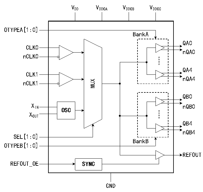
INS6310A, a versatile, low-jitter, low-power differential clock buffer, can fan out any of three input clocks to ten low-jitter differential clock outputs and one LVCMOS single-ended output. It also facilitates flexible level conversion between input and output clocks, and supports both differential and single-ended signals, and passive crystal input for input clocks.
INS6310A is a versatile, low-jitter, low-power differential clock buffer that can fan out any one of the three input clocks to ten low-jitter differential clock outputs and one LVCMOS single-ended output. It also allows flexible level conversion between the input and output clocks. The input clock supports differential signals, single-ended signals, and passive crystal input.

• Support 2 sets with 5 differential outputs (LVDS/LVPECL/HCSL/ high-impedance)
• Support 3 inputs
■ 2 differential or single-ended (DC~2500MHz), LVPECL/LVDS/CML/SSTL/HSTL/HCSL
■ 1 passive crystal or single-ended (10M~40MHz)
• Additional phase jitter: 40fs RMS(10KHz~1MHz)
80fs RMS(12KHz~20MHz)
• PSRR: -65/-76dBc(LVDS/LVPECL)@156.25MHz
• Output power: 2.5V/3.3V
• Core supply voltage: 3.3V
• Operation Temperature Range: -40℃~+85℃
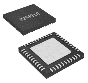
• Package: 7.0*7.0*0.8mm(QFN48)
